- 您现在的位置:买卖IC网 > Sheet目录287 > 25AA080C-I/MS (Microchip Technology)IC SRL EEPROM 1KX8 1.8V 8-MSOP
�� �
�
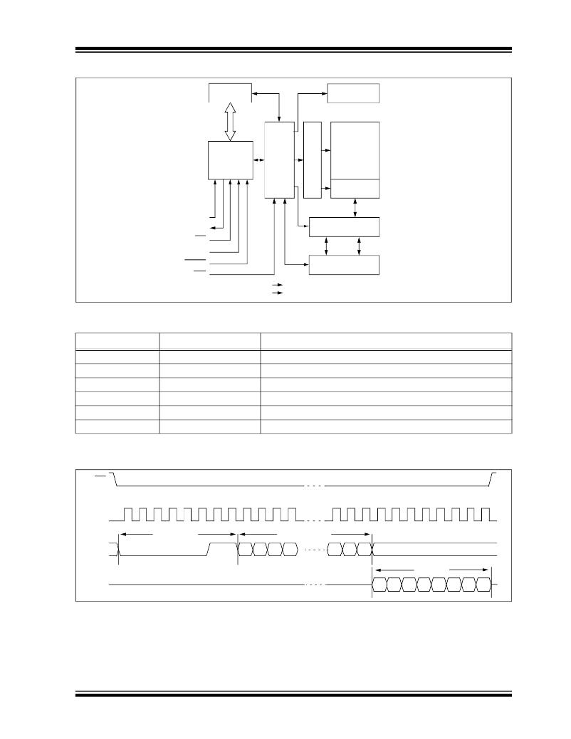
�25XX080C/D�
�Block� Diagram�
�STATUS�
�Register�
�HV� Generator�
�I/O� Control�
�Logic�
�Memory�
�Control�
�Logic�
�X�
�Dec�
�EEPROM�
�Array�
�Page� Latches�
�SI�
�SO�
�CS�
�SCK�
�HOLD�
�WP�
�V� CC�
�V� SS�
�Y� Decoder�
�Sense� Amp.�
�R/W� Control�
�TABLE� 2-1:�
�INSTRUCTION� SET�
�Instruction� Name�
�READ�
�WRITE�
�WRDI�
�WREN�
�RDSR�
�WRSR�
�Instruction� Format�
�0000� 0011�
�0000� 0010�
�0000� 0100�
�0000� 0110�
�0000� 0101�
�0000� 0001�
�Description�
�Read� data� from� memory� array� beginning� at� selected� address�
�Write� data� to� memory� array� beginning� at� selected� address�
�Reset� the� write� enable� latch� (disable� write� operations)�
�Set� the� write� enable� latch� (enable� write� operations)�
�Read� STATUS� Register�
�Write� STATUS� Register�
�FIGURE� 2-1:�
�CS�
�READ� SEQUENCE�
�0�
�1�
�2�
�3�
�4�
�5�
�6�
�7�
�8�
�9� 10� 1� 1�
�2� 1� 2� 2� 2� 3� 2� 4� 2� 5� 2� 6� 2� 7� 2� 8� 2� 9� 3� 0� 3� 1�
�SCK�
�Instruction�
�16-bit� Address�
�SI�
�0�
�0�
�0�
�0�
�0�
�0�
�1�
�1� 15� 14� 13� 12�
�2�
�1�
�0�
�High-Impedance�
�Data� Out�
�SO�
�7�
�6�
�5�
�4�
�3�
�2�
�1�
�0�
�?� 2009� Microchip� Technology� Inc.�
�DS22151A-page� 7�
�发布紧急采购,3分钟左右您将得到回复。
相关PDF资料
25AA1024T-I/MF
IC EEPROM 1MBIT 20MHZ 8DFN
25AA160C-I/P
IC SRL EEPROM 2KX8 1.8V 8-PDIP
25AA512T-I/MF
IC EEPROM 512KBIT 20MHZ 8DFN
25C040X/ST
IC EEPROM 4KBIT 3MHZ 8TSSOP
25C080-I/P
IC EEPROM 8KBIT 3MHZ 8DIP
25C320-E/P
IC EEPROM 32KBIT 3MHZ 8DIP
25LC010AT-E/MC
IC EEPROM 1KBIT 10MHZ 8DFN
25LC040AT-E/MC
IC EEPROM 4KBIT 10MHZ 8DFN
相关代理商/技术参数
25AA080C-I/P
功能描述:电可擦除可编程只读存储器 8K 1K X 8 16B PAGE 1.8V SER EE IND RoHS:否 制造商:Atmel 存储容量:2 Kbit 组织:256 B x 8 数据保留:100 yr 最大时钟频率:1000 KHz 最大工作电流:6 uA 工作电源电压:1.7 V to 5.5 V 最大工作温度:+ 85 C 安装风格:SMD/SMT 封装 / 箱体:SOIC-8
25AA080C-I/SN
功能描述:电可擦除可编程只读存储器 8K 1K X 8 16B PAGE 1.8V SER EE IND RoHS:否 制造商:Atmel 存储容量:2 Kbit 组织:256 B x 8 数据保留:100 yr 最大时钟频率:1000 KHz 最大工作电流:6 uA 工作电源电压:1.7 V to 5.5 V 最大工作温度:+ 85 C 安装风格:SMD/SMT 封装 / 箱体:SOIC-8
25AA080C-I/ST
功能描述:电可擦除可编程只读存储器 8K 1K X 8 16B PAGE 1.8V SER EE IND RoHS:否 制造商:Atmel 存储容量:2 Kbit 组织:256 B x 8 数据保留:100 yr 最大时钟频率:1000 KHz 最大工作电流:6 uA 工作电源电压:1.7 V to 5.5 V 最大工作温度:+ 85 C 安装风格:SMD/SMT 封装 / 箱体:SOIC-8
25AA080CT-E/MNY
制造商:MICROCHIP 制造商全称:Microchip Technology 功能描述:8K SPI Bus Serial EEPROM
25AA080CT-E/MS
制造商:MICROCHIP 制造商全称:Microchip Technology 功能描述:8K SPI Bus Serial EEPROM
25AA080CT-E/P
制造商:MICROCHIP 制造商全称:Microchip Technology 功能描述:8K SPI Bus Serial EEPROM
25AA080CT-E/SN
制造商:MICROCHIP 制造商全称:Microchip Technology 功能描述:8K SPI Bus Serial EEPROM
25AA080CT-E/ST
制造商:MICROCHIP 制造商全称:Microchip Technology 功能描述:8K SPI Bus Serial EEPROM